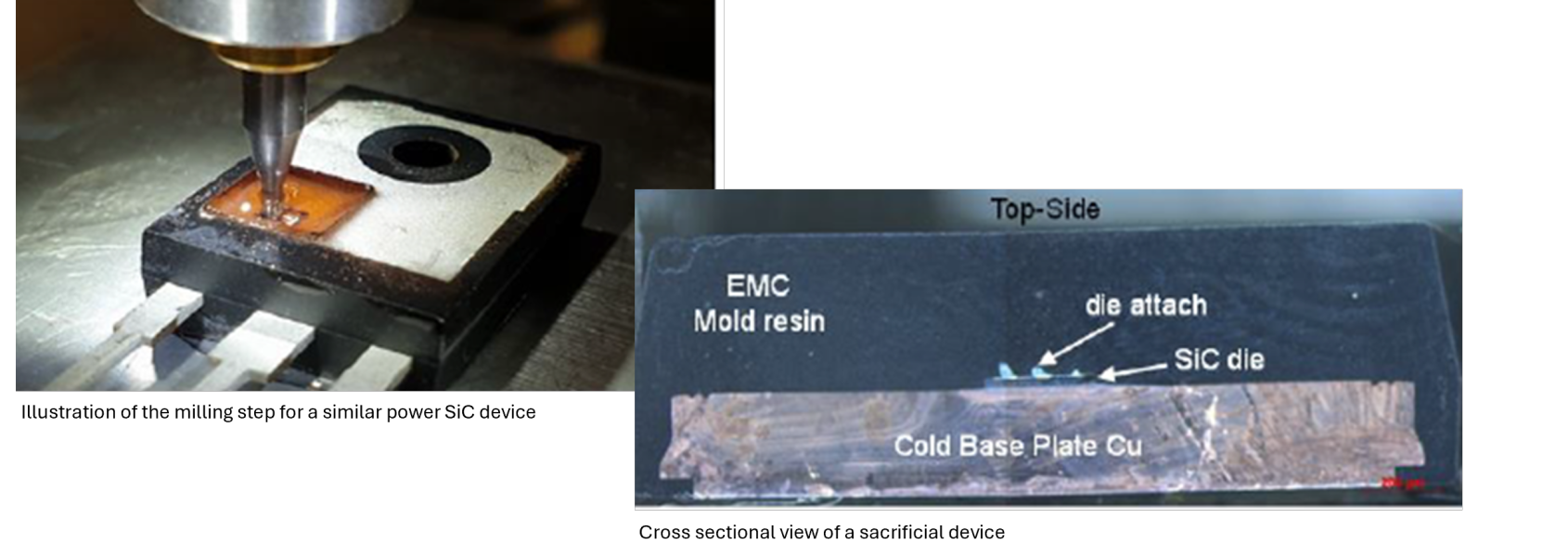


![]()
We are pleased to announce our new partnership with infinityPV - a company known for its pioneering technologies in the field of slot-die coating and roll-to-roll processing. This strategic cooperation marks an important milestone for us to jointly develop innovative products for the semiconductor industry, new energy (perovskites, fuel cells, etc.) and life science and to tap into new market potential.
Our cooperation is focused on Europe and primarily on the D-A-CH region (Germany, Austria, Switzerland), where we combine our long-standing expertise in semiconductor technology, PV, microelectronics and life science with the technological innovation of infinityPV, we are creating the basis for forward-looking solutions that combine sustainability, efficiency and quality. The focus of the cooperation is on the development and market launch of new materials and processes that will expand and optimize the range of applications in coating technology.
We look forward to working closely with the infinityPV team and to the exciting projects that lie ahead.
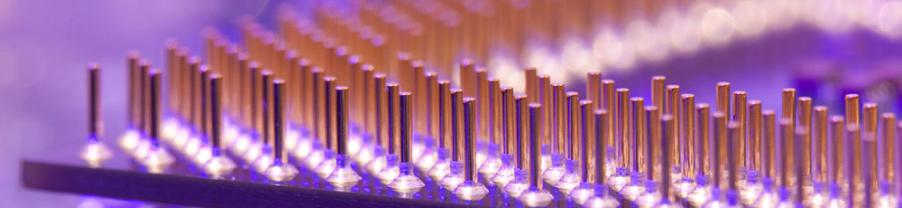
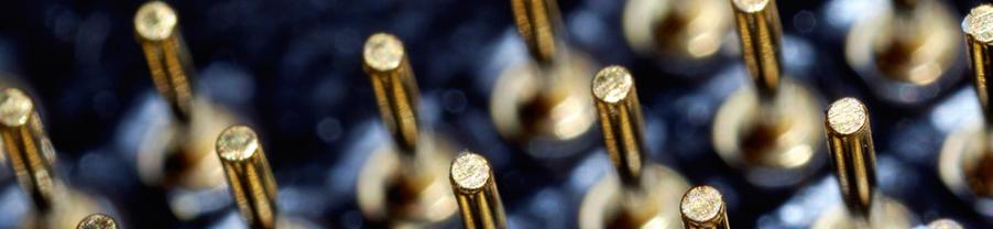
 We are deligthed at JPK Group to announce our new partnership with SOLARIUS. SOLARIUS is a leading provider of precision systems for non-contact surface inspection, measurement, analysis, and visualization. The product portfolio combines high-resolution sensors with automated data acquisition systems and powerful analysis tools. Offerings range from desktop systems for off-line inspection, to semi-automated systems for fast, precise measurements, to customized multi-station platforms for high-volume in-line inspection.Based on experience in various fields, we use this technology for Optical Probe Card Inspection. If you are either looking for cyclic routine inspection, new card income inspection or post maintenance check-up, SOLARIUS will be able to support your application request. Our target: A fast probe card inspection enabling a clear and resilient decision if a probe card is OK for testing or NOT.