You are here
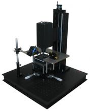
Sentris
Thermal Imaging Microscope for Semiconductor Device Failure Analysis
Due to the continued decrease in integrated circuit feature size and supply voltages, detecting and locating the miniscule amount of heat generated by failure sites has become increasingly difficult. The Sentris thermal imaging microscope pinpoints the low-level infrared thermal emissions by IC faults such as short circuits and leakage current.
Using a non-destructive testing (NDT) process called lock-in thermography, failures can be isolated on both bare (front or backside) and packaged devices and no surface coating is required. Sentris can also locate low-power fail sites on SMD components, such as capacitor leakage. The x, y position of defect sites can be located, as well as defect depth. Depth analysis can be very helpful when isolating faults in stacked die packages.
In addition to fault isolation, Sentris also includes thermal analysis tools for true temperature mapping, junction temperature measurement, die attach evaluation, and thermal resistance evaluation.
Overview
Faults Detected
- Semiconductor ESD related faults
- Leakage current and hot spots
- Resistive shorts between gate and drain
- Shorts in mold compound of packaged devices
- Latch-up sites
- Shorts in metallization
- Defective transistors and diodes
- Oxide layer breakdown
- SMD component leakage
Functional and Uncomplicated
The innovative Sentris fault isolation process was developed by Optotherm to simplify and reduce the cost of the lock-in thermography process. Traditional lock-in thermography systems include complex function generators and power supplies in order to synchronize device power with the capture of thermal images. By eliminating the need for these complicated and expensive instruments, Sentris provides a straightforward and affordable technique to semiconductor defect isolation.
Advantages Over Liquid Crystal Thermography
Liquid crystal thermography has low sensitivity, slow response, and requires the surface of devices to be coated. These systems are limited to detecting hot spots greater than 0.1°C and because they involve steady-state device powering, the heat generated by faults diffuses through semiconductor material, blurring the location of the defect source. Sentris overcomes the limitations of liquid crystal thermography. No surface coating is required, and hot spots below 0.001°C can be detected. Furthermore, high-frequency lock-in thermography minimizes heat diffusion, enabling the precise location of faults.
Compliments Other FA Tools
Semiconductor devices are becoming smaller, faster, highly integrated, and multi-functional with the result that failures often cannot be found using only one analysis technique. It is often necessary to use multiple tools to pinpoint different types of faults. Sentris thermal emission analysis is often used in conjunction with photon emission and OBIRCH analysis. Photon emission is used primarily to analyze leakage current resulting from gate oxide defects, latch-ups and ESD failures. OBIRCH is most often used to detect leakage current, short circuits and areas of high resistance.
Features and Capabilities
- High sensitivity Lock-in Thermography fault isolation
- Defect depth analysis of stacked die
- True temperature mapping using Emissivity Tables
- Visual camera probing
- Junction temperature measurement
- Bare and packaged device analysis
- Front and backside analysis
- Detection of die attach problems
- Thermal resistance evaluation
Capabilities
Lock-in Thermography Fault Isolation
Lock-in thermography is a process of automatically and repeatedly powering a device at regular intervals using a laboratory power supply and reed relays while the temperature response of the device is integrated and analyzed over time. Using this technique, hot spots that heat up less than 1mK (0.001°C) and dissipate below 100 µW can be detected.
In addition to identifying the x, y location of a defect, fault depth within a stacked-die can also be determined by analyzing the phase angle between device power and subsequent surface heating.
True Temperature Mapping
When imaging semiconductor devices, much of the contrast on the image is usually due to emissivityvariations, not to temperature variations. Measuring true temperature requires compensating for these emissivity variations according to the following procedure.
First, the unpowered device is placed on the thermal stage so that its temperature can be precisely controlled. After it has reached a stable temperature, the Emissivity Tables software tool is used to automatically create an emissivity map of the device. By applying the emissivity map to thermal images, accurate temperatures can be obtained at any point on a device.
Junction Temperature Measurement
During integrated circuit operation, internal junction self-heating leads to a large concentration of heat at the junction. The peak temperature in a device is at the junction itself and heat conducts outward from the junction into the package. For this reason, accurate junction temperature measurement during device operation is an integral part of thermal characterization. The Emissivity Tables software tool allows accurate temperature measurement of the junction by automatically compensating for emissivity variations across the die surface.
Die Attach Evaluation
Die attach defects can be due to a number of causes such as inadequate or contaminated die attach material, delamination, or voids. Sentris thermal analysis tools like Image Sequence analysis can be used to assess the flow of heat away from a device in order to determine the integrity of the die bond.
Thermal Resistance Evaluation
A common method of characterizing the thermal performance of packaged devices is using the concept of thermal resistance. Thermal resistance is the steady-state temperature rise of a device junction above the temperature of a reference point (device package or heat sink) for each watt of power dissipated in the junction. Once a device's thermal resistance is known, the junction temperature can be readily calculated using temperature measurements on the reference point. Sentris enables accurate measurement of device packaging and heat sinks for reliable thermal resistance evaluation.